Billions of people may be continuously running AI inference for their waking hours in the near future. Satisfying this demand requires relentless focus on efficiency to reduce the required quantities of two key inputs: energy and capital. The constraints on these inputs in conjunction with the slowing and/or stagnation of both Moore's Law and Dennard Scaling has left hardware architects no choice but to pursue Domain Specific Architectures (DSAs) - architectures tailored to the task at hand.
The current dominance of GPUs in modern deep learning is largely accidental - it was pure serendipity that the computational workload of graphics and deep learning were similar. Remnants of their graphical heritage still persist in GPU architectures today. What would AI inference hardware look like if it was redesigned carte blanche? By working backwards from the AI inference workload, we can determine some optimal properties these DSAs should have. Furthermore, we will attempt to predict the direction the inference paradigm will shift over time - a crucial exercise for hardware architects and engineers alike to ensure return on investment.
It's memory, not compute that matters
>90% of the total system energy is spent on memory in large ML models
— Onur Mutlu
Often times it feels like many people have a view of computing systems much like natural philosophers did prior to Copernicus — compute is like the earth, at the centre of the universe. This is a bad model for understanding AI inference.
Progress in memory latency and throughput has lagged behind Moore's law since the beginning 1.Reading and writing from memory is extraordinarily slow when compared to computation. Below is one of my favourite animations adapted from Vrushank Desai, demonstrating the latency of different operations on an A100 GPU2.
Latency and throughput isn't the only issue with memory. The one true optimization objective for any accelerator is performance per dollar, and reducing power consumption is one key way of reducing the Total Cost of Ownership (TCO). The graph below compares the energy cost of different operations on different datatypes for the Google TPU v4i 3.
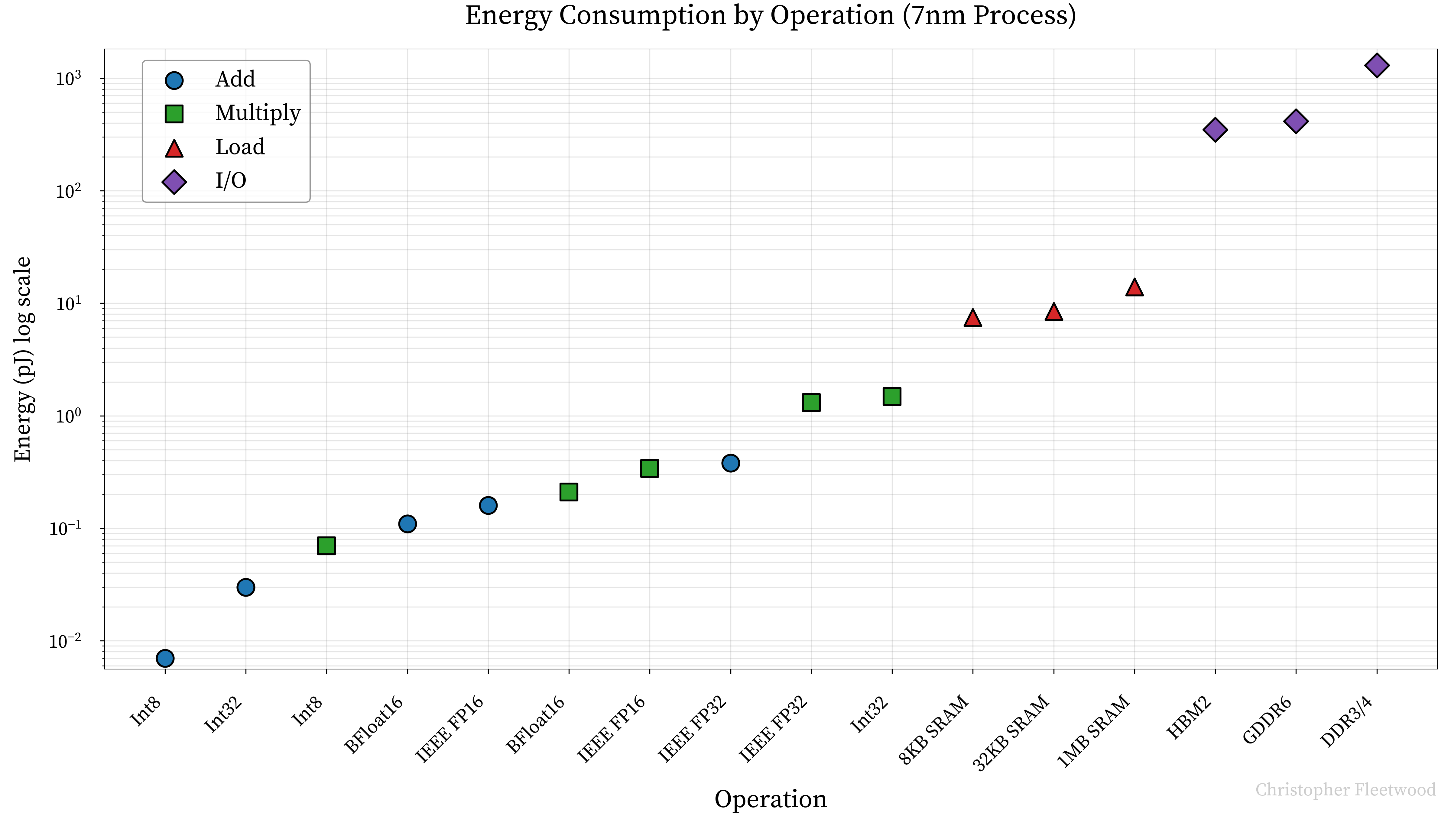
Note the log y-axis, this should highlight how incredibly energy intensive reading and writing to DRAM is, regardless of the memory standard, when compared with actual computation.
All of this together allows us to define one key property of any DSA for AI inference to decrease power consumption and improve performance — minimize data movement.
We will use this as an axiom for the remainder of the essay.
A simplified model of Transformer inference
As always, we must begin with the problem we are trying to solve, and work backwards towards our solution. We will iteratively build up a more and more detailed picture of inference in an attempt to derive optimal hardware principles.
The above animation depicts a very simple visual model of performing work on a traditional accelerator (e.g. a GPU) with different bottlenecks - try clicking on the different bound types! This simple model affords us some intuition about performing a forward pass of a transformer.
A simplified forward pass consists solely of moving extremely large, contiguous weight tensors from Global Memory (DRAM) to Shared Memory (L1 / SRAM), performing some number of operations on them in combination with our inputs, then storing the results back in DRAM.
When memory bound, we can see there are instances when the Processing Elements (PEs) are doing nothing (a.k.a stalling). When compute bound, we see the PEs cannot keep up with the data flowing through memory. As compute progress has outpaced memory progress, keeping our compute units fed is one of the core optimization principles in deep learning. Therefore, optimizing the process of moving these weight tensors to and from memory should be the underlying principle behind many of our hardware design decisions.
Lower precision
The first port of call when optimizing a piece of work is to simply try to avoid doing the work at all. One obvious way to do this is reducing the size of our weight tensors by using smaller data types. We can cut our work in half, quarters or more by representing our weights with less bits. All modern accelerators support FP8 inference, pushing into FP4 territory in the latest generation. In order to maintain numerical accuracy with lower bit widths, hardware support for high precision accumulation and online quantization is necessary. There is however another less obvious incentive for reducing the bit width of our data types.
The number of full adders that are required for multiplying two floating point numbers together is a quadratic function of the number of mantissa bits. For two floating point numbers with mantissa bits, the multiplication requires an array of full adders. This translates to 576 full adders for FP32, 121 for FP16, 64 for BF16 and 16 for FP8(E4M3) 4. Less adders per multiplier means we can fit more compute per unit area, or trade the die area for L1 cache.
These two forces together are a powerful incentive to reduce the precision of our model. Unfortunately, there are limits — how many bits does a transformer really need? Given that intelligence and compression are deeply intertwined5, we cannot expect to continue to reduce the precision of our datatypes without compromising model performance. Scaling Laws for Precision6 explores this in depth, and it seems that the optimal region sits somewhere between 7 and 8 bits.
Principle 1: Hardware support for low precision data types.
First class asynchronicity
One simple way to reduce the opportunity cost of moving a tensor from Global Memory to Shared Memory is to introduce asynchronous data movement. By implementing double buffering, the compute unit can work on one buffer while the other is being filled (skip ahead to the TPU animation below for a demonstration). The overlap of computation, memory transfers, and inter-accelerator communication is a prerequisite for optimal hardware utilization. This has been the defacto standard since the H100, and we should expect any self respecting DSAs to be designed "asynchronous-first".
Principle 2: Design for asynchronous transfers from day 1.
Dedicated hardware for memory transfers
We know that moving tensors from Global Memory to Shared Memory is a frequent operation in our forward pass. Therefore, it would be prudent to create an optimized subsystem within our hardware to expedite the transfers. Direct Memory Access allows us to move our tensors between memory spaces (be it Global Memory to Shared Memory within one accelerator, or even to the Shared Memory of another accelerator) without involving the host (read: CPU) at all. Nvidia terms their subsystem the Tensor Memory Accelerator (TMA).
It may sound ridiculous, but prior to the introduction of the TMA with the H100, Nvidia GPUs required all data to go via the registers in the journey from Global Memory and Shared Memory, like forcing a river through a hosepipe. DMA that is aware of tensor layouts and can copy both within a node and between nodes (termed Remote Direct Memory Access or RDMA) should be a principle concern for any future DSA.
Principle 3: Dedicated hardware for tensor aware memory transfers.
Optimal memory hierarchy for AI
Typically when we move data within a computing system, it travels through a multi-level cache hierarchy, with each level of the hierarchy trading off latency/throughput for size or the inverse. This is analogous to the human memory hierarchy (sensory memory, working memory and long-term memory).
The number of levels in your hierarchy and their size is a function of the expected workload with respect to two dimensions:
- Temporal Locality: If you've used a piece of data, you're likely to reuse it again soon.
- Spatial Locality: If you've used a piece of data, you're likely to access neighbouring elements.
In multiprocessor architectures, privacy and data consistency are also key considerations in cache design. For example, the H100 features an 80MB shared L2 cache that is accessible by multiple Streaming Multiprocessors (SMs), requiring sophisticated synchronization and coherency checks to maintain data consistency, which is inherently slow.
Utilizing a memory hierarchy designed for one workload will be inefficient for another. CPUs are designed for very unpredictable workloads, with random access patterns being the norm. GPUs on the other hand have threads frequently reusing data and in larger contiguous chunks. These different access patterns lend themselves to different designs, with CPUs benefiting from multiple smaller cache levels to expedite random accesses at different temporal and spatial localities. GPUs have more predictable and bulk-oriented access patterns, meaning they can effectively utilize fewer, larger cache levels. We should intuitively understand why CPUs often have a 3/4 tier cache hierarchy whereas GPUs typically have only 2 tiers.
Let's return to our simplified model and derive the optimal hierarchy for AI inference. We move weight tensors from DRAM into L1, using the whole weight tensor at ~the same time. Once we are done with that tensor, we will not use it again until the subsequent forward pass. Therefore, the idea of caching (storing data nearby for reuse) falls apart altogether. If we use a typical cache hierarchy for AI inference, we will be filling our L1/L2 with data that won't be reused any time soon.
What we really want is a high bandwidth, low latency storage space, much like L1/SRAM, but outside of the usual caching paradigm. This storage space can store chunks of our weight tensors whilst we operate on them. This is known as a scratchpad. A scratchpad negates all of the usual overheads that come with cache management, and gives us the fast working memory we need! We have now arrived at our next principle: replace your cache hierarchy with an outsized scratchpad.
In theory, if our scratchpad was large enough, we could store entire intermediate tensors between kernel invocations! This would completely remove roundtrips to Global Memory. Unfortunately, L1 is located on-chip and is implemented using SRAM which requires 6(!) transistors per bit of storage, meaning even small amounts of storage (read: kilobytes) takes an enormous amount of die area which could otherwise be used for compute. This hasn't stopped many hardware startups like Cerebras, Groq and Tenstorrent from trading off some amount of compute for cache.
Principle 4: Replace your cache hierarchy with an outsized scratchpad.
Anatomy of AI Inference
We will now focus on an algorithmic analysis of Transformer inference from a single accelerator perspective. This section is largely derived from Chapter 7 of How to scale your model7 and Transformer Inference Arithmetic8. I would recommend studying them both for a comprehensive understanding.
A modern Transformer consists of only 6 operations:
- Some form of Attention (Multi Head Attention (MHA), Grouped Query Attention (GQA) etc)
- A Feedforward Network (Mixture of Experts for frontier models)
- Root Mean Square Normalization
- An activation function (typically Swish + GLU within the FFN)
- Rotary Position Embeddings
- Addition to the residual stream
The Attention and Feedforward blocks are the most relevant when discussing performance. In an ideal world, the other operations can be fused into the aforementioned operations and thus incur ~little cost.
Inference consists of two distinct phases with very different computational requirements:
- Prefill: Processing a long initial sequence (system/user prompt) in parallel, populating the KV Cache.
- Decode: Autoregressively generating tokens using the KV Cache.
Every algorithm has a property known as the Arithmetic Intensity, which is the
ratio of operations performed to bytes accessed. The counterpart to this is
the ops:byte ratio of the hardware accelerator, which is the ratio of the
accelerators "math" bandwidth and memory bandwidth. An algorithm is compute
bound if the arithmetic intensity is higher than the accelerators ops:byte
ratio. We should endeavour to be compute bound so that our hardware is always doing useful work. Understanding the interplay between these ratios is key for performance.
| DRAM | SRAM | ||||||
|---|---|---|---|---|---|---|---|
| Hardware | FP16 TFLOPs | Size (GB) | BW (TB/s) | Ops:byte | Size (MB) | BW (TB/s) | Ops:byte |
| NVIDIA H100-SXM5 | 989 | 80 | 3.35 | 295.2 | 30.81 | 31 | 31.9 |
| NVIDIA A100 | 312 | 40 | 2.0 | 156.0 | 20.72 | ~19 | 16.4 |
| Tenstorrent Blackhole | 387 | 32 | 0.51 | 758.8 | 204.93 | 46.6 | 8.3 |
| Google TPU v4i | 138 | 8 | 0.61 | 226.2 | 144 | ~13.54 | 10.2 |
| 1 228KiB * 132 SMs, 2 192KB * 108 SMs, 3 1464KB * 140 Tensix Cores, 4Estimated | |||||||
As a mental reference point for these capacities, a matrix (e.g. Llama2 attention projections) in BF16 is 32MiB (~33.6MB). Determining if an operation is compute or memory bandwidth bound becomes quite complex, given the capacity constraints and throughput variation between the different memory spaces. Despite the difficulty, we will attempt to determine the typical boundedness of our two core operations in a transformer forward pass. This should inform the optimal balance between memory bandwidth and compute capacity.
Matrix Multiplications
Almost the entirety of the FLOPs spent on our model will be in matrix multiplications. Matrix multiplication has a very interesting property that bears repeating: the computational cost grows with the cube of the dimension , whereas the number of memory accesses grows with the square of the dimension . This means as the dimension grows the ratio of compute to data improves (from a hardware perspective).
In a transformer, matmuls occur primarily in two places:
- Attention Projections: Computing the , , and projections.
- Feedforward Networks: The large linear transformations in each FFN block.
The most common form of matmul we will perform in a forward pass is , where is the batch size, is our model dimension and is the outer dimension of the weight tensor in question. At what point does this operation become compute bound on a given accelerator?
We are looking to determine when for the following:
For our loads, we multiply each term by a factor of two as our values are 2 bytes. In order for the matmul to become compute bound on a given accelerator, the arithmetic intensity must exceed the ops:byte ratio:
As demonstrated in How to scale your model7, we can simplify the denominator to , as both and are typically much larger than . Using an Nvidia H100 as our reference, capable of 989 TFLOPs of BF16 compute with memory bandwidth of 3.35TB/s, we get the following:
This means our matmuls will only become compute bound when our . During inference, this will almost certainly occur during prefill (most system + user prompts exceed this (ignoring prompt caching)). However during decoding it will be quite the challenge to achieve this batch size.
One might think that quantizing our weights to would cut our in half, but the H100 can also perform 2x the number of FLOPS in FP8, so we are back where we started. If we wanted to lower our , what hardware changes could we make? The obvious one is to simply increase our memory bandwidth by stumping up for more advanced High Bandwidth Memory (HBM). However, this has diminishing returns with respect to our true optimization objection of performance / dollar. Another approach could be to trade off compute for SRAM as discussed earlier. In our previous table we can see that for the H100, meaning we can accommodate algorithms with much lower intensity whilst still saturating our compute.
Attention
How to scale your model7 rigorously analyses attention to determine its Arithmetic Intensity. We will summarize it here, expand with recent advancements and what implications they have for hardware.
Using FlashAttention9, the Arithmetic Intensity of a single head of (multi-headed) attention is as follows:
Where is the (existing) sequence length, is the number of tokens we are currently sampling, is the batch size and is our . During prefill , so the expression simplifies to . This is quite favourable for hardware utilization! For our H100, this means that we are compute bound if — which should be very common during prefill (e.g. a standard system prompt). Decoding however, is a different story.
During decode , and , which allows us to approximate the original expression as:
Arithmetic intensity this low means decode is fundamentally memory bound. This should make intuitive sense — we are loading a (potentially large) KV cache and performing a small number of operations due to the volume of input data (). Without some architectural modifications (e.g. MQA, GQA, MLA) to reduce the size of the cache, there isn't much we can do to improve this situation.
This makes decreasing the size of our KV cache one of our primary concerns, not only for inference performance, but also for capacity. Earlier, our simplified model assumed only weight tensors are consuming DRAM capacity. However, the size of our cache quickly becomes considerable. Let's do some napkin math using Deepseek V310 671Bs hyperparameters to demonstrate, where and . V3 didn't use MHA, so we will use a plausible value of .
In the MHA case, we store both for each layer using 2 bytes per value, meaning our cache size is as follows:
Given that a H100 has 80GB of DRAM, we will exceed the entire storage capacity once the cache hits ~46,000 tokens, just from the cache! This means naïve MHA fundamentally prohibits long context. We can see now why there has been intense optimization pressure applied to reducing the size of the KV cache - it is key for both long context conversations and inference performance. These optimizations included Multi Query Attention and Grouped Query Attention, but both methods trade model performance for cache size.
More recently Deepseek introduced Multi Latent Attention11 (MLA), with the intention of compressing the KV cache by performing a low-rank decomposition. This works well as data and computation are two sides of the same coin, and here we trade data for compute in the form of our up and down projection matrices.
For MLA, we simply store a single compressed latent for both and . Let's redo our math:
This means our KV cache is 28x smaller using MLA. Our context would need to be ~1.3M (4x the length of Ulysses) tokens before exceeding our H100 capacity. An order of magnitude difference has implications for hardware. Using MHA, we could only store 17 tokens worth of cache in SRAM on the H100, whereas with MLA we can store 492 tokens worth of cache. This means we can store entire pages of attention on-chip when using something like PagedAttention12. Much like reducing the precision of our data types, there is a lower limit here. However, I wouldn't be surprised to see inter-layer projections compressing the total cache size further.
Despite recent optimizations, we can clearly see that any single accelerator is going to be unable to accommodate a frontier model. Therefore, we must spill over from one accelerator to many.
Principle 5: For a single accelerator, turn the memory bandwidth up to 11.
Scaling out
All models being served by the frontier labs far exceed the size of a single accelerator. This necessitates sharding our model across multiple accelerators and communicating between them. Adding more chips creates a tradeoff: while it distributes both the compute and memory burden, it also increases communication overhead between chips, reducing the amount of computation available per chip to hide the communication cost. At a certain point, adding chips no longer increases performance.
Given that we want to use computation to hide communication cost, the ratio
between the number of operations we can perform to number of bytes we can send
between accelerators is important. This is known as the ops:comms ratio.
Below is a table of the ops:comms ratio for the most popular accelerators
today:
| Hardware | FP16 TFLOPs | Interconnect | Bidirectional Bandwidth (GB/s) | Ops:Comms Ratio |
|---|---|---|---|---|
| NVIDIA H100-SXM5 | 989 | NVLink 4.0 | 900 | 1099 |
| NVIDIA A100 | 312 | NVLink 3.0 | 600 | 520 |
| Tenstorrent Blackhole | 387 | Ethernet | 800 | 484 |
| Google TPU v5p | 459 | ICI | 600 | 765 |
Different sharding strategies incur different communication costs. Determining at which point an accelerator becomes communication bound for a given strategy is quite involved. Luckily for us, How to scale your model7 derives useful heuristics we can use to get an idea of when modern transformers may become communication bound, and use it to inform our hardware design.
We will restrict our analysis to the decoding phase for brevity. During decode we can only use Model Parallelism for sharding our model. At what point do we become bottlenecked by communication? To simplify the problem, we reduce our forward pass to a stack of MLPs. We consider 1D Model Parallelism for an MLP layer where we perform an AllGather on the input activations and a ReduceScatter on the output activations as shown here. We want to understand at what point , for our MLP performing the following:
Where is our batch dimension, is our model dimension, is our FFN dimension and denotes sharding.
Given that we perform 2 matmuls, each performing FLOPs, and we communicate 2 matrices of size , our and are as follows:
Where is the number of accelerators, is the per accelerator FLOPs and is our bandwidth. As we want to know when , this simplifies down to:
Astute readers will notice that is our ops:comms ratio! This formula is quite handy. Using from Deepseek V3, we can see that we become communication bound on an H100 at ~16 GPUs. If we had a more
favourable ops:comms ratio, we could scale our tensor parallelism further. This analysis neglects latency, which can dominate communication time when the volume of data transferred is low, please refer to Transformer Inference Arithmetic8 for a more thorough
treatment.
We will now briefly cover Expert Parallelism (EP), as Mixture of Expert (MOE) models are the standard for frontier models today and it has implications for hardware design. In Expert Parallelism, we dedicate an accelerator to hosting one or more experts (a specialized FFN). When processing a batch of tokens, we must send each of the tokens to a different subset of experts, depending on the result of our routing mechanism. The result from our subset of activated experts then must be aggregated afterwards. This warrants an AllToAll communication "primitive":
AllToAll is also known as a resharding operation, as we have a batch of tokens sharded in the batch dimension (our batch entries are entirely independent which is good for sharding), and we reshard them based on the result of our routing mechanism. You can imagine this as matrices flying all over to different accelerators, which necessitates a low latency, high throughput communication fabric. Given that we are performing the same communication primitives repeatedly, we should explore specialized hardware subsystems to optimize their performance.
The Deepseek V3 paper highlights the need for hardware optimizations for communications. In lieu of vendor provided hardware optimizations, Deepseek "specialized" 20/132 SMs specifically for communications. This includes performing reduce operations for the MOE AllToAll aggregation, managing memory layout of tensors being transferred between experts etc. These SMs are designed to do computation, not network management, and by specializing them for communications, not matrix multiplication, 15% of all Tensor Cores are wasted.
We should expect any performant domain specific architecture to have dedicated hardware for managing communications. It would be ideal if during data transfers the data could be transformed (e.g. arriving at the destination reduced, transposed etc). Remote Direct Memory Access (RDMA) being able to perform some primitive operations is suitably biomimetic — axons in the brain aren't just passive transmission channels, but perform "diverse functional operations" 13 beyond mere signal propagation.
Principle 6: Design for scale-out from day 1.
Principle 7: Dedicated communication hardware should complement compute hardware.
Implications of test time compute scaling
By now we have analysed today's state of the art. Unfortunately, the paradigm does not stand still whilst we are designing hardware. Recent advancements in test time compute scaling have been called "the next scaling law", as demonstrated by the OpenAI O series. There are 2 dimensions in which we can scale inference compute: serially and parallel.
Scaling inference compute serially manifests as extended multi step reasoning chains, analogous to Kahneman's System 2 thinking. This is opposed to saying the first thing off the top of your head (System 1). In contrast, scaling inference computation in parallel is like having clones approach the same problem, with each potentially landing at different places in the solution space.
Scaling in the serial dimension (massively) increases demand for inference, in particular the decoding phase. As we determined earlier, attention during decode is inherently memory bound (MLA notwithstanding) without high batch sizes. This may contribute to something like "economies of scale" for providers that can hit high numbers of concurrent users.
Scaling in parallel is more nuanced. As we stated earlier, we can only reach high utilization of our hardware during decode when our batch size is high (), which is not always easy to achieve even in a serving setting using Continuous Batching14. To reiterate: given that we must pay the fixed cost of moving the weights from memory, low batch sizes have low Arithmetic Intensity and therefore do not utilize our hardware effectively. Now that scaling in parallel has been shown to increase response quality, we can run our serving infrastructure and achieve higher utilization by simply padding our batches with more parallel chains of thought. The users get an improved experience that can be delivered for free.
I expect research into the optimal trade off between these 2 scaling dimensions to be a hot topic this year, resulting in "token optimal inference time scaling". This closely mirrors the exploration-exploitation dilemma.
Summary
Using multiple different approaches, we've derived a (non-exhaustive) list of design decisions that should hold for any AI inference accelerator, namely:
- Hardware support for low precision data types
- Design for asynchronous transfers from day 1
- Dedicated hardware for tensor aware memory transfers
- Replace your cache hierarchy with an outsized scratchpad
- For a single accelerator, turn the memory bandwidth up to 11
- Design for scale-out from day 1
- Dedicated communication hardware should complement compute hardware
Domain Specific Architectures
With an understanding of the inference workload, we can now explore some domain specific architectures and determine if they adhere to the design principles we derived.
Google TPU
The Google TPU is one of the most successful DSAs in the history of computing. It would be derivative to explore the architecture in detail, particularly as Google has been open about the design across the generations15, 16. In brief, the TPU adheres to all of the principles we have previously outlined, which is why it is currently the leading accelerator on a performance / dollar basis, our one true optimization objective.
Instead, we will focus on one of the most interesting components of the TPU - the Systolic array. A systolic array is a special purpose compute unit designed to accelerate certain regular computations, popularized by H.T Kung17, who rediscovered systolic arrays in 1982 (It’s important to be the last person to discover something). Its ability to accelerate matrix multiplications makes it a popular choice for AI inference accelerators.
The TPUv2 onwards features one or more 128x128 weight stationary systolic arrays. They take their fitting name from the similarity to the human circulatory system. Data (blood) passes through many processing elements (cells) before returning to memory (heart).
The above animation shows a 4x4 weight stationary systolic array, a scaled down version of the unit in the TPU, performing a matrix multiplication (). Weights are preloaded into the processing elements, and the output is accumulated from left to right.
The principle benefit of these units is minimizing data movement to the theoretical limit. A naïve square matrix multiplication performs memory reads, and has a space complexity of . This can be improved with tiling, using tiles of size to , where is the size of the cache line and is the total size of the cache in bytes. A systolic array further improves this to the optimal number of memory reads of . In theory, each element of the input and weights is read only once, and is used many times as it flows through the array. In practice this is not the case, given that you have a fixed dimension for your systolic array and a dynamic workload consisting of many problem sizes. Even if the array is only partially utilised, the entire unit must do work, which can harm power efficiency. Furthermore, keeping the systolic array fed requires complex hardware and software infrastructure.
Do we see the theoretical efficiency gains from a systolic array play out in practice? The TPUv4 uses 1.3x-1.9x less power than its generational counterpart the A100. The systolic array is a staple for any hardware startup looking to build an AI accelerator, including OpenAI, who are reported to be taping out their new systolic array based accelerator this year.
Tenstorrent
Tenstorrent is a startup founded in 2016 with the ambitious goal of creating an AI accelerator and supporting software stack from scratch capable of competing with Nvidia. Their upcoming accelerator, Blackhole, offers an excellent case study in how the principles we've derived might be implemented in practice.
Architecture
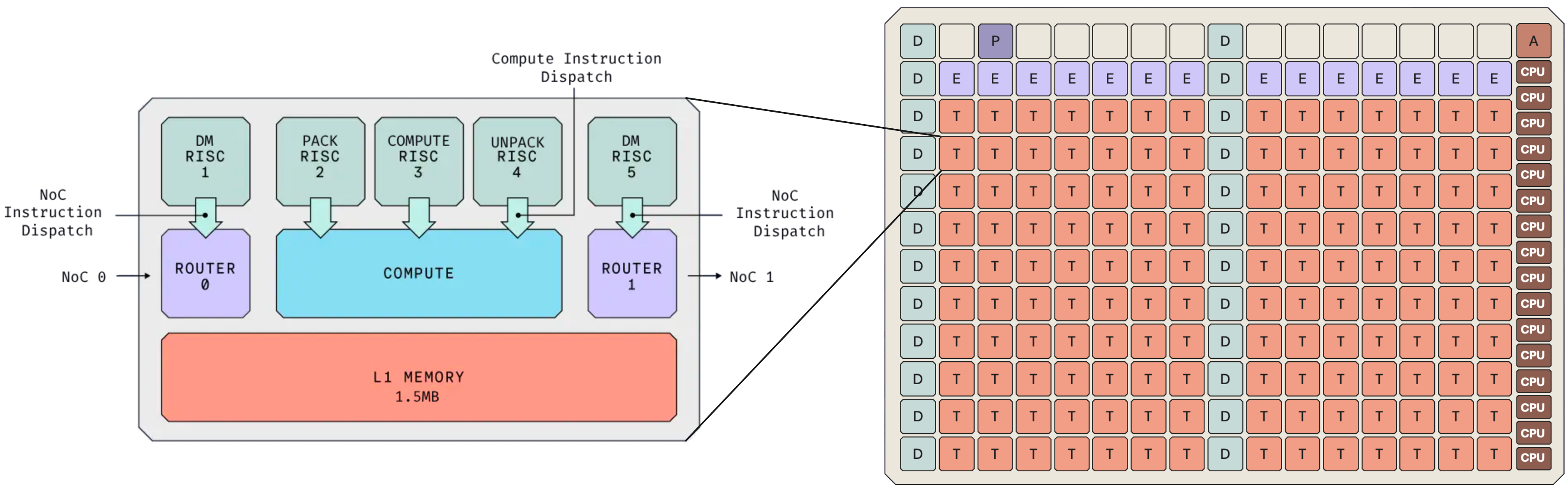
Blackhole's layout should feel familiar to those who have seen that of a GPU, with a grid of independent cores. However, the resemblance is only surface level. We can see that the chip features families of specialized cores, namely D for data movement, T for Tensix (compute), E for Ethernet, CPU cores for running Linux, and some additional cores for board management. This specialization embodies our principle of optimized hardware subsystems for their intended functions.
The Tensix core, analogous to Nvidia's Streaming Multiprocessor, serves as the fundamental compute unit. Each Tensix core contains:
- Two data movement cores, designed for initiating and managing asynchronous transactions on the Network on Chip (NoC) - directly implementing our "asynchronous first" principle.
- 1.5MB of fast local SRAM - adhering to our scratchpad principle.
- A 32×32 (reminiscent of OpenAI's Triton) matrix tile engine, analogous to Nvidia's Tensor Cores.
- Three compute cores, two specialized for packing and unpacking data types - aligning with our "hardware support for low precision datatypes" principle.
The NoC connects the entire grid of cores together, allowing cores to copy data between each other and across the ethernet network to any other accelerator. This is the underlying thesis behind Tenstorrent: cost-effective accelerators with massive high bandwidth scale out.
Supporting this architecture is a novel software stack that represents a departure from traditional programming models. Unlike CUDA, where Shared Memory/L1 is undefined between kernel invocations, Tenstorrent's architecture allows intermediate results to remain in L1 and undergo successive transformations. This approach is almost systolic in nature: designed for repeated transformations before returning to memory — strongly adhering to our core principle of minimizing data movement.
The GDDR6 Gambit
The most controversial design choice for Blackhole is the refusal to use High Bandwidth Memory. Tenstorrent has opted to use GDDR6 for Blackhole with a bandwidth of only 512GB/s — contrast this with the H100 with 3.35TB/s. The CEO, Jim Keller, has stated that HBM is too expensive for the accelerators to hit commodity pricing. How accurate really is this?
According to Tae Kim of Barrons, the total bill of materials (BOM) for a H100 was $3320 in 2023. Combining this with the figure of $15/GB from SemiAnalysis for the HBM3 memory, the memory contributes ~36% of the overall BOM of the H100. GDDR6 is far cheaper than HBM.
By leveraging an outsized L1, asynchronous transfers, the NoC, and a more flexible programming model, Tenstorrent is hoping that they don't need HBM. The winds of AI architecture do seem to be blowing in their favour. The introduction of MLA have shown that attention may not be forever memory bound. Furthermore, if they can crack low latency, high bandwidth interconnect, then the burden of loading model parameters can be distributed across accelerators as follows:
Where is our model parameters, is our number of accelerators and is our memory bandwidth.
Challenges
Tenstorrent still has huge challenges ahead of them, the largest of which being software. The "CUDA moat" is usually the first topic of discussion when disparaging any hardware upstart. The moat as it's commonly understood is the maturity and (relative) robustness of the CUDA software stack. However, the real moat is the 1000's of engineers worldwide who have internalized the SIMT paradigm. Developing an entire software stack from zero, transparently scaling it out to 1000s of accelerators and forcing engineers to trade SIMT for MIMD may be a bridge too far.
Furthermore, Nvidia is now royally flush with cash, sitting with ~$38B of cash equivalents as of Q3 2024, and this industry is extremely capital intensive. This is primarily a problem for 2 reasons:
- Nvidia is capable of reserving the cream of the crop when it comes to process nodes.
- If the paradigm trends more memory bound, not less, Nvidia is first in line for HBM4e onwards.
However, if Tenstorrent can pull off a solid software stack in the next ~24 months and AI architecture trends continue to move in their favour, they'll be a strong contender.
Skate to where the puck is going
The iteration time for designing and fabricating a new chip is typically 2-3 years. The AI paradigm has been moving much faster than this, with new architectures and datatypes being created on an increasing cadence. This is a huge problem for hardware architects, as you may end up with hardware optimized for the models of yesteryear. If you're a hyperscaler spending $80B on hardware and the paradigm shifts dramatically before the 3 years required to recoup your costs3, well you're out of luck! Whilst no one can concretely predict future architectural advances, is there any way we can gain some semblance of directionality of the paradigm in order to derisk our investments?
If we believe that the search space of possible methods for constructing AGI is "large and sparse", then it would be prudent to take inspiration from our only existence proof: the human brain. In his remarkably prescient talk from 2010, Demis Hassabis outlines an iterative approach to developing the components of AGI via Systems Neuroscience.
Systems neuroscience does not mindlessly mimic the brain, but attempts to understand/extract the underlying algorithms and creatively and pragmatically reimplement them in software and hardware. He further explores this argument in a 2017 paper18, highlighting parallels between previous AI innovations and their counterparts in the brain. These aren't coincidental similarities, but rather convergent evolution toward optimal solutions in the landscape of intelligence.
Hassabis' thesis has continued to hold true. Frontier models are now all Mixture of Experts, which exhibit the same regional specialization we see in the brain. Looking forward through this lens, what other biological analogues could we see be implemented in-silico? I would hazard a guess at episodic memory systems and something similar to the hippocampal-neocortical consolidation system.
Hardware startups
The growth in demand for AI inference will not abate for the foreseeable future. Hardware architects attempting to hedge their bets when designing inference hardware in this market will almost certainly fail. Given that from specialisation comes efficiency, and flexibility and specialisation are diametrically opposed, one must be bold and bet on the way the winds of AI architecture will blow. Luckily, systems neuroscience can give us a lens through which to attempt to peer into the future.
This principle of bold specialization extends beyond just startups. Every programmer is effectively an investor — their time and expertise are their capital. Being an early adopter of a technology that goes on to succeed can pay huge dividends, but this requires the same willingness to make bold, calculated bets on specific technological directions rather than hedging as a generalist.
The principles we've derived: minimizing data movement, optimizing memory hierarchies, and designing for scale-out — provide a roadmap for those willing to make such bets in the inference hardware space. It remains to be seen if there exists a David to take down Goliath.
Thanks to Erik Kaunismäki, Madeline Ephgrave, Luca Peric and Amine Dirhoussi for their insightful feedback on this post. Thanks to Felix LeClair and Martin Chang for their corrections.
Resources
- Stanford Seminar on H100
- Compute Substrate for Software 2.0 (2021)
- Mitigating bottlenecks on Coral TPU
- Data movement is all you need
- VLIW lecture @ ETH Zurich
- Systolic lecture ETH Zurich
- NVIDIA Deep Learning Performance guide
- Roofline model
- Systolic arrays
- Tim Dettmers on overtraining and data types
- Corsix blog on Tenstorrent
- Hopper architecture in depth
- Nvidia GPU performance guide
- TPU pipelining
- Cache complexity of matrix multiplication
- Serve in what you train
- HBM cost analysis
- TPU Hotchips (systolic array)
- MLA from Epoch
- Batching effects on GPT
- Flash Attention 1
- TPUv4i SRAM
Footnotes
-
D Patterson. (2004), "Latency lags bandwith", https://dl.acm.org/doi/10.1145/1022594.1022596 ↩
-
H Abdelkhalik et al. (2022), "Demystifying the Nvidia Ampere Architecture through Microbenchmarking and Instruction-level Analysis", https://arxiv.org/pdf/2208.11174 ↩
-
Jouppi et al. (2021), "Ten Lessons From Three Generations Shaped Google’s TPUv4i", https://gwern.net/doc/ai/scaling/hardware/2021-jouppi.pdf ↩ ↩2
-
J Dean. (2019), "The Deep Learning Revolution and Its Implications for Computer Architecture and Chip Design", https://arxiv.org/pdf/1911.05289 ↩
-
Legg, S et al. "Universal intelligence: A definition of machine intelligence.", https://arxiv.org/pdf/0712.3329 ↩
-
Kumar et al. (2024), "Scaling Laws for Precision", https://arxiv.org/pdf/2411.04330 ↩
-
Austin et al. (2025), "How to Scale Your Model", https://jax-ml.github.io/scaling-book ↩ ↩2 ↩3 ↩4
-
Chen, Carol. (2022), "Transformer Inference Arithmetic", https://kipp.ly/blog/transformer-inference-arithmetic/ ↩ ↩2
-
T Dao et al. (2022), "Flashattention: Fast and memory-efficient exact attention with io-awareness", https://arxiv.org/pdf/2205.14135 ↩
-
Liu, Aixin, et al. "Deepseek-v3 technical report.", https://arxiv.org/abs/2412.19437 ↩
-
Liu, Aixin, et al. "Deepseek-v2: A strong, economical, and efficient mixture-of-experts language model.", https://arxiv.org/pdf/2405.04434 ↩
-
W Kwon et al. (2023), "Efficient Memory Management for Large Language Model Serving with PagedAttention", https://arxiv.org/pdf/2309.06180 ↩
-
Sasaki, T. (2013), "The axon as a unique computational unit in neurons", https://pubmed.ncbi.nlm.nih.gov/23298528/ ↩
-
Yu, Gyeong-In, et al. "Orca: A distributed serving system for Transformer-Based generative models.", https://www.usenix.org/system/files/osdi22-yu.pdf ↩
-
Jouppi et al. (2017), "In-Datacenter Performance Analysis of a Tensor Processing Unit", https://arxiv.org/abs/1704.04760 ↩
-
Jouppi et al. (2021), "Ten Lessons From Three Generations Shaped Google’s TPUv4i", https://gwern.net/doc/ai/scaling/hardware/2021-jouppi.pdf ↩
-
H.T Kung. (1982), "Why Systolic Architectures", https://www.eecs.harvard.edu/~htk/publication/1982-kung-why-systolic-architecture.pdf ↩
-
Hassabis et al. "Neuroscience-inspired artificial intelligence.", https://pubmed.ncbi.nlm.nih.gov/28728020/ ↩